Blog
Mastering Hardware: My Nand2Tetris Journey Begins

In 2010 a man named Maurice Wilkes died. His death was a loss to the computer industry as he was considered one of the last people who truly understood hardware and software at a fundamental level. I have worked exclusively with software for my entire career, but I have always tried to expand my knowledge circle wider than my specific area of expertise. As such, I have always tried to be interested in learning more about hardware, but often lacked the time to get into it—that and not having an idea of where to start.
Enter Nand2Tetris, a course on coursera.org by Noam Nisan and Shimon Schocken. I first learned about this course a few years ago when a good friend introduced it to me. I quickly jumped in but gave up after a few weeks. Over the years, I have started—and abandoned—it several times. Finally, In January 2023 I decided to commit to completing the course. By March I had finished part one, complete with certificate and a healthy feeling of accomplishment.
I want to make it clear that I found this course incredibly worth it. Up to then my understanding of how memory and a CPU worked was rudimentary, but this course not only explained them, but it also saw me building them myself. If you have ever wanted to know what your computer is doing at the hardware level, I highly recommend this course. It pulls back the curtain on what is going on inside just about every device you use today and lets you peek inside the magical ‘black box’.
The course
The full course (over two parts), as the name suggests, starts with the humble NAND gate, and takes you on a journey through hardware and software until you can write a complete game of Tetris on the virtual hardware you created. I think this is what drew me to the course. It felt like making bread from scratch, but instead of buying the ingredients, I was growing the wheat and raising the chickens for the eggs and cows for the milk. There is something quite ‘fundamental’ in building a system from scratch.
We live in a world that feels like it is speeding up all the time. There is precious little time to stop and understand something before you must implement it and move on to the next thing. Having just come from studying for (and completing) a CKAD exam, I decided I wanted to learn something for me. I actively chose to slow down and take the time to do this course. So, on a rainy Saturday afternoon, I sat down and began the course that would change how I perceive hardware forever.
Some caveats before we continue, though. While you do not have to have an existing knowledge of hardware, an idea of logic gates and how they work will make understanding the material much easier. You should also know how to code in a language that allows you to read file paths from the command line (e.g., Python, Ruby, Java). As far as what you can expect to get out of this course—in one word: knowledge. Read further to decide if you want to take the same journey.
NAND
The first thing I had to learn was what a NAND gate is:
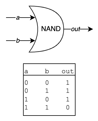
Above is a diagram of a NAND gate and accompanying truth table—a table that shows all possible combinations of input and output values. We know that performing And logic where one of the operands is 0 results in a 0 output. Only when both inputs are 1, is the output also a 1. A NAND gate work the opposite.
For the purposes of the course, NAND would function as the indivisible starting point and building block for all the other logic gates and components I would create.
Boolean Logic
The first section of the course was about using NAND to create the most common ‘primitive’ gates.
NOT
For instance, I created a NOT gate by feeding its single input (in) to both the a and b inputs of a NAND gate, and the output was exactly the behaviour of a NOT gate. Below is a diagram of what I mean:
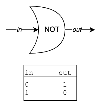
A NOT gate works by ‘flipping’ its input to the opposite. If you look at the truth table of the NAND gate, you see that when a and b are both 0, the output is 1 and when they are both 1, the output is 0.
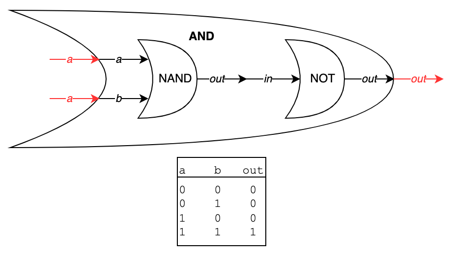
AND
This was my first revelation—that each logic gate is its own little ‘black box’, made up of other gates. The AND gate, as another example, is built from a NAND gate and a NOT gate (which itself is built from a NAND gate). The NAND gate does its thing, then acts as a NOT to flip the result and you get AND. The eye opener was that every CPU in existence, at its lowest level, comes down a complex dance of such gates processing signals.
The actual work of building the gates was done in a Hardware Description Language, like the ones used in the industry, just much simpler. The course comes with the necessary Java-based tools to build and test these gates.
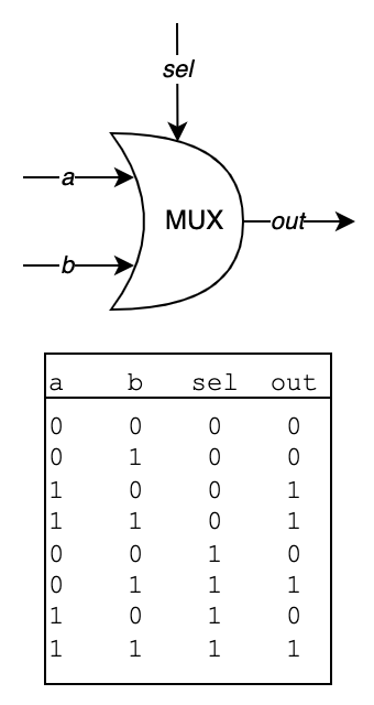
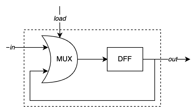
MUX
I was most fascinated by the MUX and DMUX gates. Here is an explanation of the MUX (Multiplexor) chip to give you an idea. It has three inputs: a and b and a selector. You feed two values in (e.g., 0 and 1) and, depending on what value you chose for the selector (0 or 1), either the a input (0) or the b input (1) is fed to out. That is how it appears on the outside: values flow in, you pull a lever and one of those values flows out. But that is not what is really happening; when you look inside the box, it is just the accumulated gates, wired up in the correct order that give the illusion of flow. It is the same way 60 still images per second gives the illusion of movement.
I am reminded of the quote by the Canadian computer scientist Alfred Aho: “Computer Science is a science of abstraction—creating the right model for a problem and devising the appropriate mechanizable techniques to solve it.” You use the black boxes you created in the previous stage to help build the ones you will use in the next stage—black boxes within black boxes.
Boolean Arithmetic
In this section, I used the gates I had designed previously to construct a Half Adder, a simple chip with two inputs (a and b) and two outputs (sum and carry). What it does is ‘add’ the two inputs and, if the result is more that 1, the sum is 0 and the carry bit is 1 (the concept is the same as adding decimal numbers). This bit would then carry over from the ‘1’ column in a binary value to the ‘2’ column. So, if you added 1 and 1, you would get 10 (two).
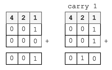
Again, here was the illusion at work. Bits appeared to combine and produce values and carry overs, but it is just the clever implementation of a XOR gate and an AND gate.

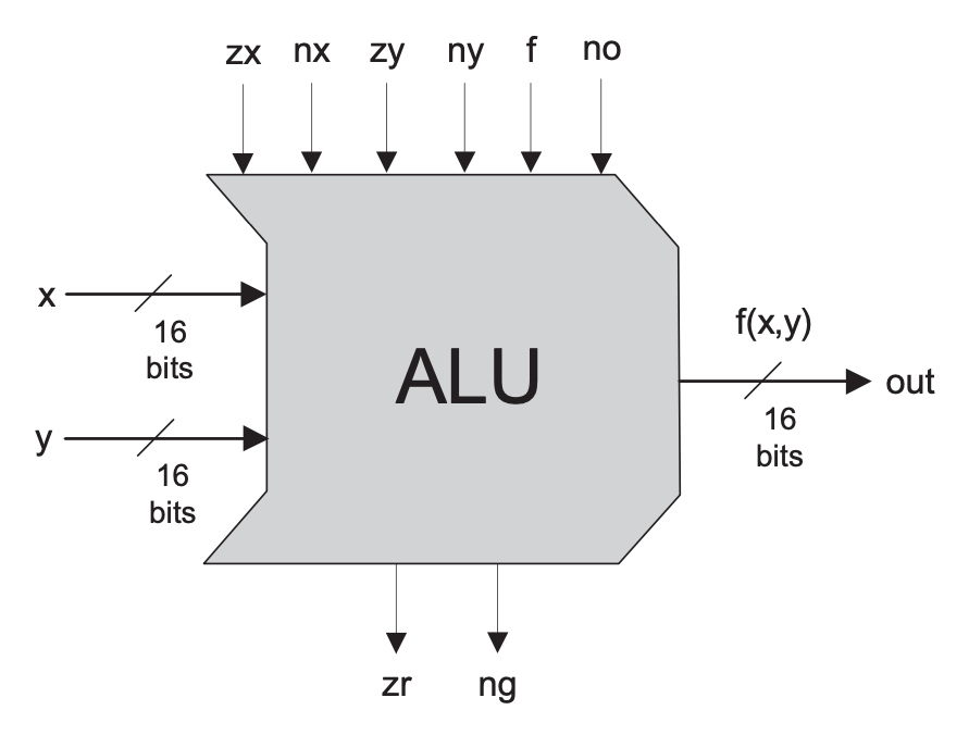
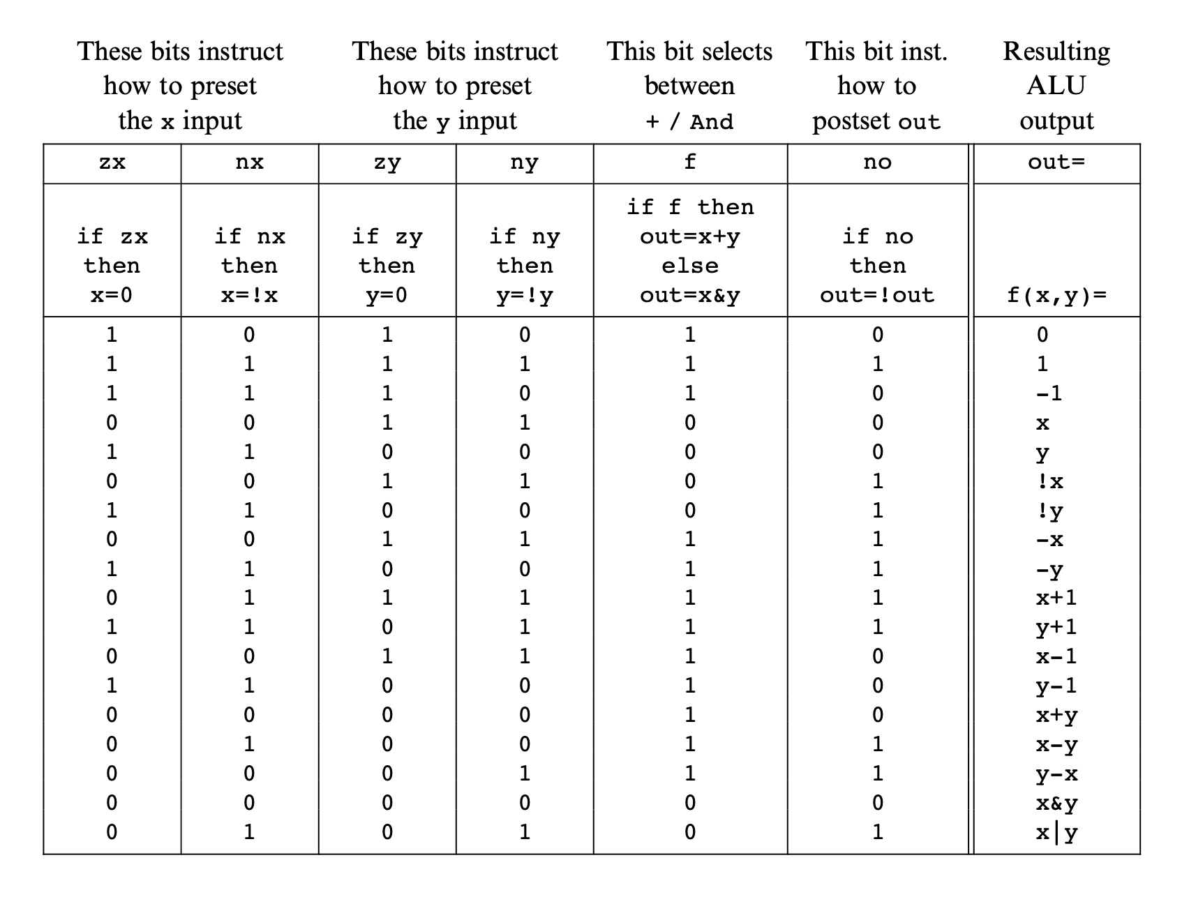
The culmination of the section was the ALU (Arithmetic Logic Unit), a complex little chip that performs a range of mathematical and logic operations on two inputs. Like the MUX chip, you feed in two values, flip a few control bits, and out pops the result. Abstractions on top of abstractions, on top of abstractions.
Sequential Logic
Thus far these chips had been working instantly—I fed in some input and immediately out came the result. But this is not representative of reality; in the real world there is time. And, in fact, without time we would not have memory. This section introduced the Data Flip-Flop (DFF), the second (and last) primitive gate. Its output is its input from one ‘tick’ earlier (ticks are how many operations a CPU can perform per second—a 2GHz CPU ticks 2 billion times a second).
From this I created Bit chips and, from those, the actual memory chips. A Bit is a component made up of a MUX chip and a DFF chip that, when combined, can be given a value as input (0 or 1) and, depending on the load bit, will either load in the value you supplied or feed its own output back to itself, thus ‘remembering’ its state. This formed the basis for creating all the memory chips of this section.
What amazed me about this section was visualising how memory works, how each bit is reminding itself of its value billions of times a second!

Machine Language
The next section gave me a small break from the hardware and introduced me to assemble code. I have always wanted to learn an assembly language, but I just never actually got around to it. Here I was able to not only learn an (albeit simple) assembly language, but to also understand it.
The assembly language used in the course is called Hack and, while simple, it is very powerful. Using its syntax, it is possible to create loops, compare values and jump to other parts of the code.
As an example, to store the value 17 in the first memory register you would write:
@17
D=A
@M=D
What this code does is:
- Set the address register (A) to 17. This register serves two purposes: accessing memory addresses and setting immediate (literal) values.
- Move that value into the data register (D).
- With the value safely stored, I shift my focus to the first (0th) memory register. To do this, I set the A register to 0. The memory register (M) now points to the memory location 0.
- By setting M=D, I place the value 17 into memory register 0.
Effectively I have run a command like the following pseudocode. I just had to code each individual step of the operation.
M[0] = 17This is what every CPU is doing billions of times a second. Despite more registers and cache, modern CPUs essentially shuffle values, executing basic elements of larger calculations.
Binary
What this section taught me is how the individual binary instructions direct the computer. The following binary strings set the A register to 18 (the memory location of the target instruction). They then tell the CPU to compare the D register to the value 0. If D equals 0, jumps to that point in memory.
0000000000010010  // @18
1110001100000010  // D;JEQ
Freaky stuff. I could now read binary. I understood why assembly is not portable between CPUs. This is a literal (and custom) instruction set for this specific CPU.

Computer Architecture
After that brief detour, it was back to the hardware. The penultimate section was where I took all the hardware I had created and assembled it into a working computer. This involved mixing a variety of chips and registers and the ALU to form the CPU. These were then combined with the memory to store the program and its running values. In addition, it added a screen to the mix. Interestingly, a screen is basically memory, too. This screen is black and white, where 0 represents a black pixel and 1 is a white pixel. The keyboard is also a memory device, but a read-only one.
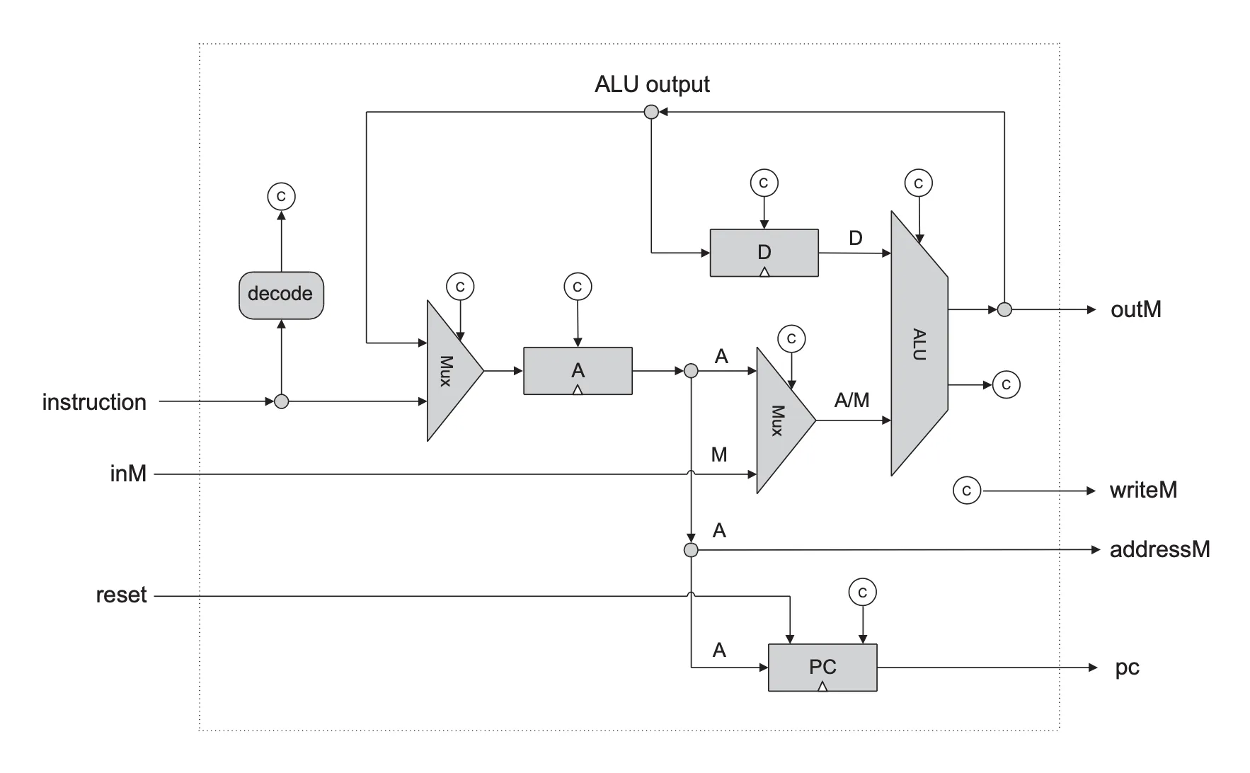
With that done, I had a complete working computer, with a CPU whose workings I could hold in my head. I could now sit with binary instructions written on a piece of paper and ‘run’ the CPU in my head.

Assembler
The final section was all about the software. This was where my programming skills came into play. I wrote an assembler in Python that turned the Hack assembly language into the binary that the CPU uses.
At this point I could write (almost) any program in the assembly language. What was more, if I wanted, I could extend the language and create new shorthand instructions in the assembly code. All I had to do was invent a new ‘shortcut’ instruction and generate the necessary sequence of binary lines.
Conclusion
And that was that: I had completed the course and I had the certificate to show for it. Was it worth it? Absolutely. I had gained the insights and perspectives into computer hardware that I had wanted for years.
The course is well-constructed, introducing a few concepts at a time and building on each section in the next one. I am not a ‘hardware’ person, but I found I was able to wrap my head around the concepts.
I had wanted to do this course for a few years, and I am now so glad I did. The journey was genuinely engaging and not some dry course given by dispassionate lecturers. I am now halfway through the second half of the course, which focuses on the software side. I will write about it when I have finished it.
If I have piqued your interest at all, I encourage you to give it a try. Like me, it may take you a few attempts, but it is well worth it.
Happy Nanding!
Written by
Jeffrey Zaayman
Our Ideas
Explore More Blogs


What Intrinsic motivation drives your colleagues with Moving Motivators
What intrinsic motivation drivers are amongst your coworkers? People are the most critical part of an organization, and managers must do all they can...
Irene de Kok


Contact